- HOME
- Technical Information
- Commissioned Analysis and Research
- spherical aberration corrected Scanning Transmission Electron Microscope:Cs-corrected STEM
spherical aberration corrected Scanning Transmission Electron Microscope:Cs-corrected STEM
What’s the aberration correction function?
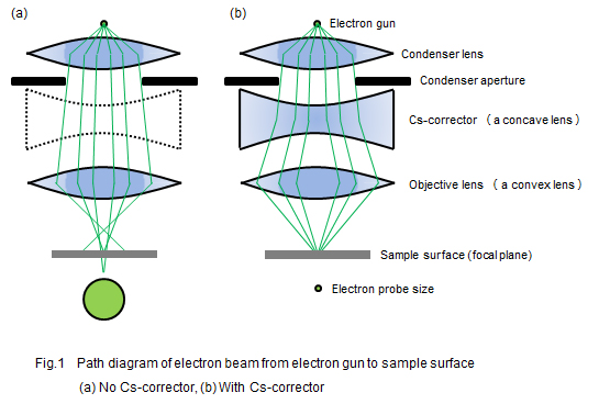
Transmission electron microscopy (TEM) has made remarkable progress due to the development of aberration correction technology nowadays. In principle, only convex lenses can be made for the magnetic field lenses used in electron microscopes. Therefore, the resolution was limited by various aberrations of the lens, especially the third-order spherical aberration (Cs). However, in recent years, a device (Cs-corrector) has been developed that realizes a concave lens using the theoretically proposed multipoles. The devices made it possible to improve lens aberration by combining a concave lens and a convex lens like an optical microscope. By incorporating this Cs-corrector into the systems of the TEM, a resolution of 0.1 nm, which could not be achieved with the conventional TEM, was achieved. Cs-corrected STEM can locate and identify elements at the single atom level.
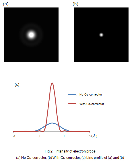
Fig. 1 shows the difference in the electron beam path diagram with and without the aberration correction mechanism in the probe system. Electron beams passing away from the center of the lens are refracted to a greater extent, so the electron beam does not normally converge to a single point on the sample surface, and the electron probe size expands. On the other hand, if a concave lens (Cs-corrector) is introduced below the convex lens, this difference in the amount of refraction can be successfully counteracted. Therefore, the electron beam can be focused to a more localized area on the sample surface, and a narrow electron probe can be formed. As shown in Fig. 2, the current value of the electron probe after aberration correction increases by about one order of magnitude compared to that before aberration correction.
High resolution STEM observation using aberration-corrected probe
The resolution of a scanning transmission electron microscope (STEM) image depends on the electron probe size. It is possible to form a narrow electron probe than before and achieve STEM observation with ultra-high spatial resolution of 0.1 nm or less using Cs-corrector. In addition, the Cs corrector has the advantage of increasing the intensity of the electron probe. As a result, a low-noise STEM image can be acquired in about 1/10 of the conventional time, and the effect of sample drift can be reduced.
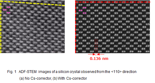
Fig. 1 shows a high-angle annular dark-field STEM (HAADF-STEM) image of a silicon crystal observed from the <110> direction with Cs-corrector or not. In the image of Fig. 1(a), the rows of silicon atoms with a spacing of 0.136 nm (silicon dumbbells) are observed only as a single bright spot (ellipse), but in the image of Fig. 1(b), these rows of atoms can be observed separately. In the image of Fig. 1(a), the atomic planes of silicon shown by the yellow dotted lines are not orthogonal to each other due to the effect of sample drift because of the long acquisition time required. On the other hand, as shown Fig, 1(b), the red dotted lines are almost orthogonal because the image can be acquired in a short time, and the deviations from the actual crystal structure are suppressed.
High energy resolution EELS using Cold-FEG
Each electron emitted from an electron source has a slightly fluctuating energy value. Furthermore, the energy distribution of the incident electron beam is affected by the stability of the system, such as high pressure and lens system, which leads to a decrease in the energy resolution of the EELS spectrum. In recent instrument systems with increased stability, the fluctuation of electron energy is largely dependent on the type of electron source. The Schottky field-emission electron gun (Schottky-FEG), which is used in most electron microscopes, requires the filament to be heated to a high temperature during use. While the cold-cathode field-emission electron gun (Cold-FEG) operates at room temperature, thus reducing the thermal fluctuation of electron energy. As a result, the full width at half maximum (FWHM) of the incident electron beam energy distribution is about 0.35 eV, which is less than half that of the Schottky-FEG.
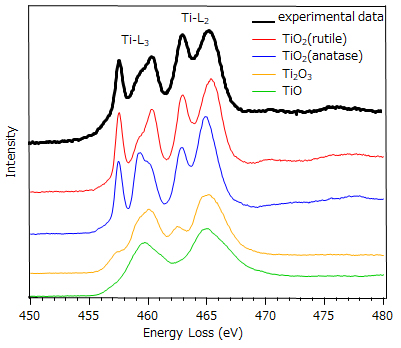
Fig. 1 shows the EELS spectra near the Ti-L edge of various titanium oxides with different structures and compositions. The EELS spectrum obtained in the experiment shows good agreement with the EELS spectrum of rutile TiO2, which identifies the measured sample as rutile TiO2.
High-sensitivity EDX measurement using a large-aperture SDD detector
Si (Li-diffusion) type semiconductor detectors (Solid State Detector: SSD) have been used as EDX detectors. The recently developed Silicon Drift Detector (SDD) is a detector that efficiently directs electrons generated in the detector by characteristic X-rays incident on the detector to the anode by applying a concentric potential gradient. The detection efficiency of the SDD detector is more than 10 times higher than that of the SSD detector. The SDD detector installed in the new system has an effective aperture of 100 mm2, which is three to four times larger than conventional detectors and enables highly sensitive EDX measurements.
Fig. 1 shows a comparison of the Two-dimensional elemental mappings of the MOS gate obtained with the SSD and SDD detectors. These results show that the SDD detector provides data with almost the same signal-to-noise ratio in 1/10 of the measurement time of the SSD detector. In addition, light elements such as C, N, and O can be clearly identified due to the improved resolution, especially in the low energy region.
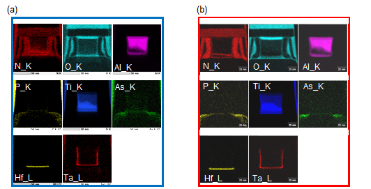
(a) When using SSD detector (measurement time 200 minutes)
(b) When using SDD detector (measurement time 20 minutes)
Measurement of carbon materials by low acceleration voltage
Carbon nanomaterials such as a carbon nanotube and a graphene, as well as organic materials, are susceptible to knock-on damage in which incident electrons directly knock atoms out of the sample. Therefore, it is difficult to perform clear structural observation and compositional analysis at the commonly used acceleration voltage of 200 kV. By observing these materials at a low acceleration voltage of 80 kV, it is possible to reduce knock-on damage caused by electron irradiation and do measurements. Fig. 1(a) and (b) show bright-field STEM and HAADF-STEM images of double-walled carbon nanotubes obtained at an accelerating voltage of 80 kV, respectively. Fig.1(c) shows the EELS spectra obtained from the measurement points A (outer layer), B (inner layer), and C (center of the nanotube). Different shapes of spectra are acquired for each measurement point, which enables us to discuss the local electronic state of carbon atoms.
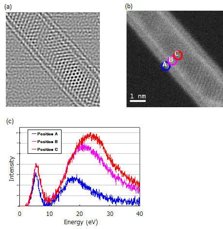
(a) A BF-STEM image (after filtering)
(b) A HAADF-STEM image
(c) EELS spectra obtained from each measurement point